Wafer production is a complex process. To test them, probe needlesmust be guided to contact pads that measure mere micrometers on aside. The controls for this process have to meet extreme demands forEMC protection and reliability. Cascade probed the market for anoptimal solution – and found It at B&R.
What do a multi-function oven, a digital clock, a toaster and a GPS navigation device have in common? Simple: they all rely on tiny integrated circuits, or microchips. In today's consumer market, it's almost a challenge to find a product that doesn't have some sort of electronics in it. Wafer production is a complex process. To test them, probe pins must be guided to contact pads that measure mere micrometers on a side. The controls for this process have to meet extreme demands for EMC protection and reliability. Cascade probed the market for an optimal solution – and found it.
The huge bandwidth of applications presents a substantial challenge for developers of semiconductor components. They face constant pressure to integrate an growing range of functions on ever smaller ships, while at the same time reducing production costs.
Already, the smartwatch on your wrist is both cheaper and more powerful than the office PC you used only 10 years ago. Thin slices of semiconductor material – known as wafers – contain more than 1,000 chips with billions of transistors and other components and currently measure up to 300 millimeters in diameter. This complexity makes developing and validating new designs and production methods a very involved process. Nevertheless, the amount of time allotted for development is shrinking rapidly.

Thorough testing ensures quality
To validate the functionality of newly developed components and ensure consistent quality once they reach series production, wafers are subjected to extensive testing in probe stations immediately after they are produced. Each wafer is fed into a measurement chamber, fastened into position with micrometer precision using a chuck and brought to a specific temperature. Then, pins are guided to specially designated contact points on the chip.
External measurement and testing instrumentation, which itself can fill entire control cabinets, dictate the positions based on the test program and then initiate the measurements. Testing is performed at temperatures ranging from -55°C to 300°C. Depending on the application, the currents measured can range from several femtoamps (a number with 15 zeros after the decimal point, or 6,250 electrons per second) up to 400 amps. It's not uncommon to have measurement frequencies in the gigahertz range – on chips used in vehicle-interval radar systems, for example – or to measure charge/discharge capacitance values as low as several femtofarads. A prominent feature of the requirements specifications is therefore the exclusion of all sources of electromagnetic interference.
High-tech measurement chamber prevents interference during testing
Cascade Microtech GmbH, a subsidiary of Cascade Microtech Inc. with headquarters in Beaverton (USA), is no stranger to these requirements. As a worldwide leading manufacturer of wafer probing solutions, the company first introduced its patented probing station in 1992 and has been improving it ever since. With over 50 years of experience developing precision positioning technology, mastery of the processes involved is an integral part of day-to-day operations.
"Under the given conditions, there are a multitude of factors to be considered in order to guide the probe pins to the contact pads, which measure a mere 30 micrometers on a side," explains Dr. Jörg Kiesewetter. Kiesewetter is the R&D manager for probe systems at Cascade Microtech's Dresden office. Here, 140 employees develop and build these systems for more than 800 customers around the world, including semiconductor producers such as IBM, Intel and Infinion, as well as many organizations like the Interuniversity Microelectronics Center (IMEC), Europe's largest research center for nano- and microelectronics.
Precision positioning
When it comes to achieving the necessary precision, the experts at Cascade Microtech have a number of mechanical and electrical tricks up their sleeves – as evidenced by their impressive 190 patents. For example, several of the 25 axes for the cross table, digital camera and other auxiliary equipment require cooling. "It's not possible to measure the quality of chip contact directly," Kiesewetter points out, "so it's essential that this process is intrinsically reliable." A single positioning error of only a few micrometers could render an entire wafer or a pin card with over 10,000 contacts unusable. This would lead to hundreds of thousands of euros in damages, not to mention tarnishing the company's reputation. Yet the requirements continue to intensify rapidly. "The contact pads occupy valuable surface area, so they are being made smaller all the time. Soon they will be 20 micrometers on a side – less than a quarter of the cross-section of a human hair." On top of that are the numerous special requests posed by device users. To keep pace with the mounting requirements, Cascade Microtech began evaluation of a new controller design concept.

"The complete modularity we have gained has helped us reduce development times considerably," reports Kiesewetter. "Outstanding support from B&R's expert engineers in Leipzig saved us valuable time." Dr. Jörg Kiesewetter, R&D Manger, Cascade Microtech
Modularity accelerates development
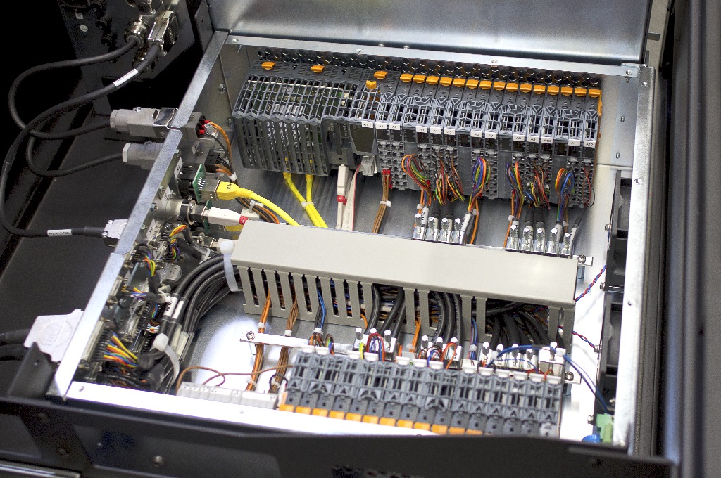
In addition to long-term product availability, EMC protection and access to a global sales and support network, the modularity of the control system was a key criteria. It would also be necessary to continue development of existing C++ program code. B&R offered the most compelling solution, and Cascade Microtech already has plans to implement it in additional devices. The designers were free to decide whether to use DC or stepper motors for the various motion control tasks. Using B&R's Generic Motion Control software solution for axis control allowed Cascade Microtech to keep hardware and software separate and accommodate different types of motors without requiring any code changes. "The complete modularity we have gained has helped us reduce development times considerably," reports Kiesewetter. "Outstanding support from B&R's expert engineers in Leipzig saved us valuable time."